- 您现在的位置:买卖IC网 > Sheet目录337 > LH28F320SKTD-ZR (Sharp Microelectronics)IC FLASH 32MBIT 70NS 48TSOP
�� �
�
�LHF32KZR�
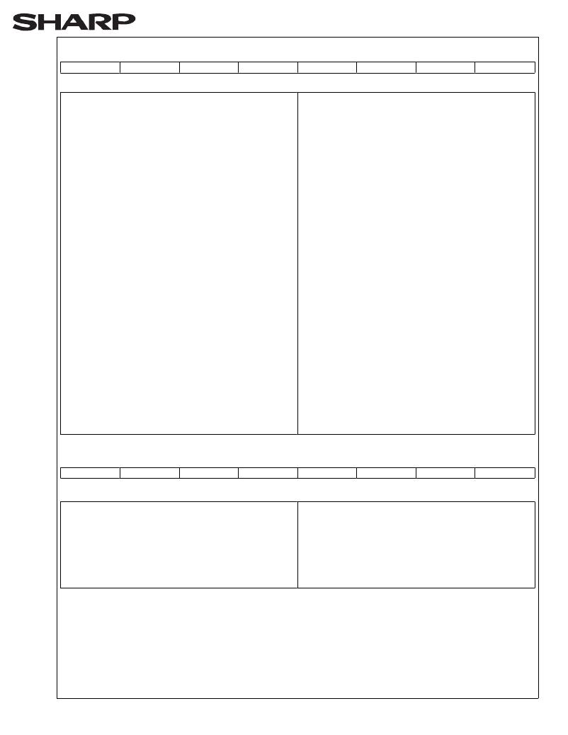
�Table� 14.� Status� Register� Definition�
�23�
�WSMS�
�7�
�BESS�
�6�
�ECBLBS�
�5�
�WSBLBS�
�4�
�VPPS�
�3�
�WSS�
�2�
�DPS�
�1�
�R�
�0�
�NOTES:�
�SR.7� =� WRITE� STATE� MACHINE� STATUS�
�1� =� Ready�
�0� =� Busy�
�SR.6� =� BLOCK� ERASE� SUSPEND� STATUS�
�1� =� Block� Erase� Suspended�
�0� =� Block� Erase� in� Progress/Completed�
�SR.5� =� ERASE� AND� CLEAR� BLOCK� LOCK-BITS�
�STATUS�
�1� =� Error� in� Erase� or� Clear� Blocl� Lock-Bits�
�0� =� Successful� Erase� or� Clear� Block� Lock-Bits�
�SR.4� =� WRITE� AND� SET� BLOCK� LOCK-BIT� STATUS�
�1� =� Error� in� Write� or� Set� Block� Lock-Bit�
�0� =� Successful� Write� or� Set� Block� Lock-Bit�
�SR.3� =� V� PP� STATUS�
�1� =� V� PP� Low� Detect,� Operation� Abort�
�0� =� V� PP� OK�
�SR.2� =� WRITE� SUSPEND� STATUS�
�1� =� Write� Suspended�
�0� =� Write� in� Progress/Completed�
�SR.1� =� DEVICE� PROTECT� STATUS�
�1� =� Block� Lock-Bit� and/or� WP#� Lock� Detected,�
�Operation� Abort�
�0� =� Unlock�
�Check� STS� or� SR.7� to� determine� block� erase,� bank�
�erase,� (multi)� word/byte� write� or� block� lock-bit�
�configuration� completion.�
�SR.6-0� are� invalid� while� SR.7="0".�
�If� both� SR.5� and� SR.4� are� "1"s� after� a� block� erase,� bank�
�erase,� (multi)� word/byte� write,� block� lock-bit�
�configuration� or� STS� configuration� attempt,� an� improper�
�command� sequence� was� entered.�
�SR.3� does� not� provide� a� continuous� indication� of� V� PP�
�level.� The� WSM� interrogates� and� indicates� the� V� PP� level�
�only� after� block� erase,� bank� erase,� (multi)� word/byte�
�write� or� block� lock-bit� configuration� command�
�sequences.� SR.3� is� not� guaranteed� to� reports� accurate�
�feedback� only� when� V� PP� ≠� V� PPH1/2/3� .�
�SR.1� does� not� provide� a� continuous� indication� of� block�
�lock-bit� values.� The� WSM� interrogates� block� lock-bit,�
�and� WP#� only� after� block� erase,� bank� erase,� (multi)�
�word/byte� write� or� block� lock-bit� configuration� command�
�sequences.� It� informs� the� system,� depending� on� the�
�attempted� operation,� if� the� block� lock-bit� is� set� and/or�
�WP#� is� not� V� IH� .� Reading� the� block� lock� configuration�
�codes� after� writing� the� Read� Identifier� Codes� command�
�indicates� block� lock-bit� status.�
�SR.0� is� reserved� for� future� use� and� should� be� masked�
�out� when� polling� the� status� register.�
�SR.0� =� RESERVED� FOR� FUTURE� ENHANCEMENTS�
�Table� 14.1.� Extended� Status� Register� Definition�
�SMS�
�7�
�R�
�6�
�R�
�5�
�R�
�4�
�R�
�3�
�R�
�2�
�R�
�1�
�R�
�0�
�NOTES:�
�XSR.7� =� STATE� MACHINE� STATUS�
�1� =� Multi� Word/Byte� Write� available�
�0� =� Multi� Word/Byte� Write� not� available�
�After� issue� a� Multi� Word/Byte� Write� command:� XSR.7�
�indicates� that� a� next� Multi� Word/Byte� Write� command� is�
�available.�
�XSR.6-0=RESERVED� FOR� FUTURE� ENHANCEMENTS�
�XSR.6-0� is� reserved� for� future� use� and� should� be�
�masked� out� when� polling� the� extended� status� register.�
�发布紧急采购,3分钟左右您将得到回复。
相关PDF资料
LHF00L28
IC FLASH 16MBIT 70NS 48TSOP
LPM409 CHASSIS
STNRD 4SLOT CHASSIS W/INPUT LEAD
LS15RB1201J04
POE SPLITTER 10.8W 12V @0.9A
LT1932ES6#TRMPBF
IC LED DRIVR WHITE BCKLGT TSOT-6
LT1937ES5#TRMPBF
IC LED DRIVR WHITE BCKLGT TSOT-5
LT3003EMSE#TRPBF
IC LED DRIVER BALLASTER 10-MSOP
LT3465AES6#TRMPBF
IC LED DRIVR WHITE BCKLGT TSOT-6
LT3466EDD-1#PBF
IC LED DRIVR WHITE BCKLGT 10-DFN
相关代理商/技术参数
LH28F400BG
制造商:SHARP 制造商全称:Sharp Electrionic Components 功能描述:4M-BIT(256KBx16) SmartVoltage Flash MEMORY
LH28F400BGB-BL12
制造商:未知厂家 制造商全称:未知厂家 功能描述:x16 Flash EEPROM
LH28F400BGB-BL85
制造商:未知厂家 制造商全称:未知厂家 功能描述:x16 Flash EEPROM
LH28F400BGB-TL12
制造商:未知厂家 制造商全称:未知厂家 功能描述:x16 Flash EEPROM
LH28F400BGB-TL85
制造商:未知厂家 制造商全称:未知厂家 功能描述:x16 Flash EEPROM
LH28F400BGE-BL12
制造商:未知厂家 制造商全称:未知厂家 功能描述:x16 Flash EEPROM
LH28F400BGE-BL85
制造商:未知厂家 制造商全称:未知厂家 功能描述:x16 Flash EEPROM
LH28F400BGE-TL12
制造商:未知厂家 制造商全称:未知厂家 功能描述:x16 Flash EEPROM